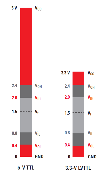
The figure above shows the respective voltage levels of a TTLand a LVTTL signaling interfaces using colored bars.
Driver output
At the low logic level, the driver guarantees an output voltage within the bottom red window.
| ● | The maximum driver output voltage, namely VOL is 0.4 V for both TTL and LVTTL. |
| ● | The minimum driver output voltage is GND |
At the high logic level, the driver output voltage is within the upper red window.
| ● | The minimum driver output voltage, namely VOH is 2.4 V for both TTL and LVTTL. |
| ● | The maximum driver output voltage is VCC: 5 V for TTL and 3.3 V for LVTTL |
Receiver input
The receiver guarantees to see a low logic level when the input signal voltage is within the bottom red and dark gray windows.
| ● | The maximum receiver input voltage, namely VIL is 0.8 V for both TTL and LVTTL. |
| ● | The minimum receiver input voltage is GND |
The receiver guarantees to see a high logic level when the input signal voltage is within the upper red and dark gray windows.
| ● | The minimum receiver input voltage, namely VIH is 2.0 V for both TTL and LVTTL. |
| ● | The maximum receiver input voltage is VCC: 5 V for TTL and 3.3 V for LVTTL |
The dark gray window is a 0.4 V noise margin between the driver output and the receiver input.
The light gray window is an area where the receiver cannot guarantee the logic level.
Typically the actual transition Vt between logic level low and high will occur at around 1.5 V but the actual Vt level may change a lot according to specimens or process (P) variations, actual Vcc supply voltage (V), and temperature (T). Only VIL and VIH are guaranteed over P,V,T variations.